If you need urgent consulting help click here
STM32F103 Mini
Overview
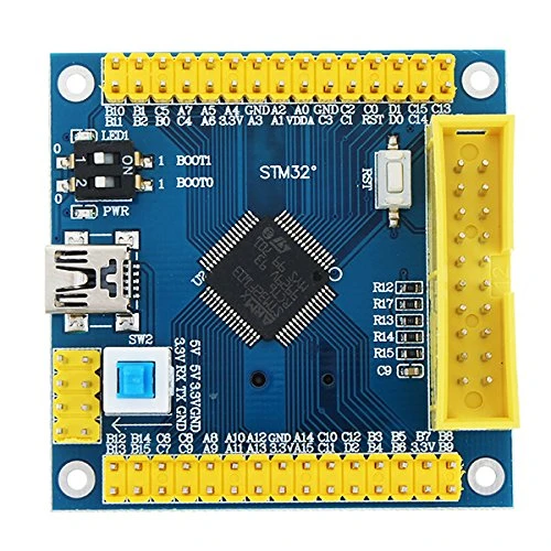
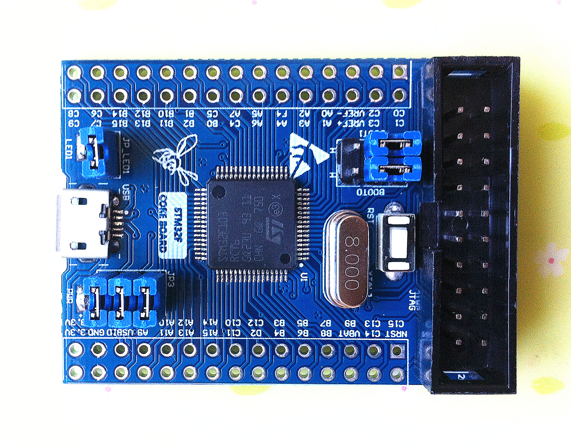
The STM32F103_MINI board features an ARM Cortex-M3 based STM32F103RC MCU
with a wide range of connectivity support and configurations. There are
multiple version of this board like stm32f103_mini.


Hardware
STM32F103 Mini provides the following hardware components:
STM32 microcontroller in QFP64 package
Flexible board power supply:
USB VBUS or external source (3.3V, 5V, 7 - 12V)
Power management access point
Two LEDs:
User LED (LD1), power LED (LD2)
USB re-enumeration capability:
Mass storage
More information about STM32F103RC can be found here:
Supported Features
The Zephyr stm32f103_mini board configuration supports the following hardware features:
Interface |
Controller |
Driver/Component |
|---|---|---|
NVIC |
on-chip |
nested vector interrupt controller |
UART |
on-chip |
serial port-polling; serial port-interrupt |
PINMUX |
on-chip |
pinmux |
GPIO |
on-chip |
gpio |
CLOCK |
on-chip |
reset and clock control |
FLASH |
on-chip |
flash memory |
WATCHDOG |
on-chip |
independent watchdog |
ADC |
on-chip |
ADC Controller |
PWM |
on-chip |
pwm |
SPI |
on-chip |
spi |
USB |
on-chip |
USB device |
Other hardware features are not yet supported in this Zephyr port.
The default configuration can be found in the defconfig file:
boards/arm/stm32f103_mini/stm32f103_mini_defconfig
Connections and IOs
Each of the GPIO pins can be configured by software as output (push-pull or open-drain), as input (with or without pull-up or pull-down), or as peripheral alternate function. Most of the GPIO pins are shared with digital or analog alternate functions. All GPIOs are high current capable except for analog inputs.
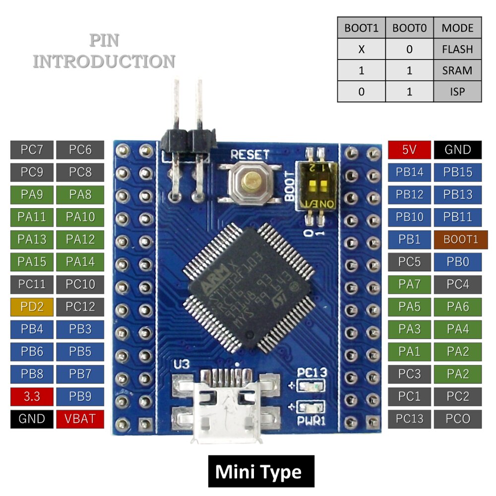
Board connectors:

Default Zephyr Peripheral Mapping:
UART_1 TX/RX: PA9/PA10
UART_2 TX/RX: PA2/PA3 (ST-Link Virtual COM Port)
SPI1 NSS/SCK/MISO/MOSI: PA4/PA5/PA6/PA7
SPI2 NSS/SCK/MISO/MOSI: PB12/PB13/PB14/PB15
I2C1 SDA/SCL: PB9/PB8
PWM1_CH1: PA8
USER_PB: PC13
LD1: PA5
USB_DC DM/DP: PA11/PA12
System Clock
The on-board 8MHz crystal is used to produce a 72MHz system clock with PLL.
Programming and Debugging
Applications for the stm32f103_mini board configuration can be built and
flashed in the usual way (see Building an Application and
Run an Application for more details).
Flashing
There are 2 main entry points for flashing STM32F1X SoCs, one using the ROM bootloader, and another by using the SWD debug port (which requires additional hardware such as ST-Link). Flashing using the ROM bootloader requires a special activation pattern, which can be triggered by using the BOOT0 pin.
